
The global transition toward renewable energy has placed solar technology at the centre of efforts to reduce dependence on fossil fuels. Yet despite rapid progress in photovoltaic research, scientists continue to search for materials that can deliver higher efficiency, greater stability, and lower environmental impact. A recent study led by Ms. Sweety Chauhan under the supervision of Dr. Anuj K. Sharma and Dr. Nitin Singha at the National Institute of Technology Delhi, India, offers a new direction. Published in the Journal of Electronic Materials, the research examines how replacing a commonly used component in solar cells could dramatically improve performance and durability.
The paper, titled “Sb₂S₃ as Hole Transport Layer Material Massively Enhances the Performance and Stability of Tin Based Perovskite Solar Cell,” investigates a new design for lead-free perovskite solar cells. By incorporating the inorganic material antimony trisulfide (Sb₂S₃) into the device structure, the researchers demonstrate, through numerical simulation, that solar cell efficiency could increase significantly while also improving long-term stability.
Perovskite solar cells are widely considered one of the most promising next-generation photovoltaic technologies. Their exceptional optoelectronic properties and relatively low manufacturing costs have already enabled rapid improvements in solar energy conversion. However, many of the most efficient designs still rely on materials that pose environmental or stability challenges. The study, therefore, explores how strategic material substitution could address these limitations while preserving high efficiency.
The challenge of building better solar cells
Solar cells operate through the photovoltaic effect, a process in which incident sunlight generates electron-hole pairs within a semiconductor material. These charge carriers are then separated and transported through specialised layers within the device to produce an electrical current. Modern photovoltaic devices rely on carefully engineered structures that optimise light absorption, charge separation and carrier transport.
Traditional silicon-based solar cells dominate the commercial market, but they require energy-intensive manufacturing and relatively expensive fabrication processes. Researchers have therefore increasingly turned their attention to emerging photovoltaic technologies such as copper indium gallium selenide, copper zinc tin sulphide and particularly perovskite solar cells. These materials exhibit high absorption coefficients, tunable band gaps, and efficient charge-transport properties, making them attractive candidates for next-generation solar energy systems.
Perovskite materials typically follow an ABX3 crystal structure in which different ions occupy specific lattice positions. Hybrid organic-inorganic perovskites based on lead halides have delivered remarkable power conversion efficiencies in recent years. Yet the presence of lead introduces concerns about toxicity and environmental safety. For this reason, researchers have explored alternative compositions that eliminate lead while maintaining favourable electronic properties.
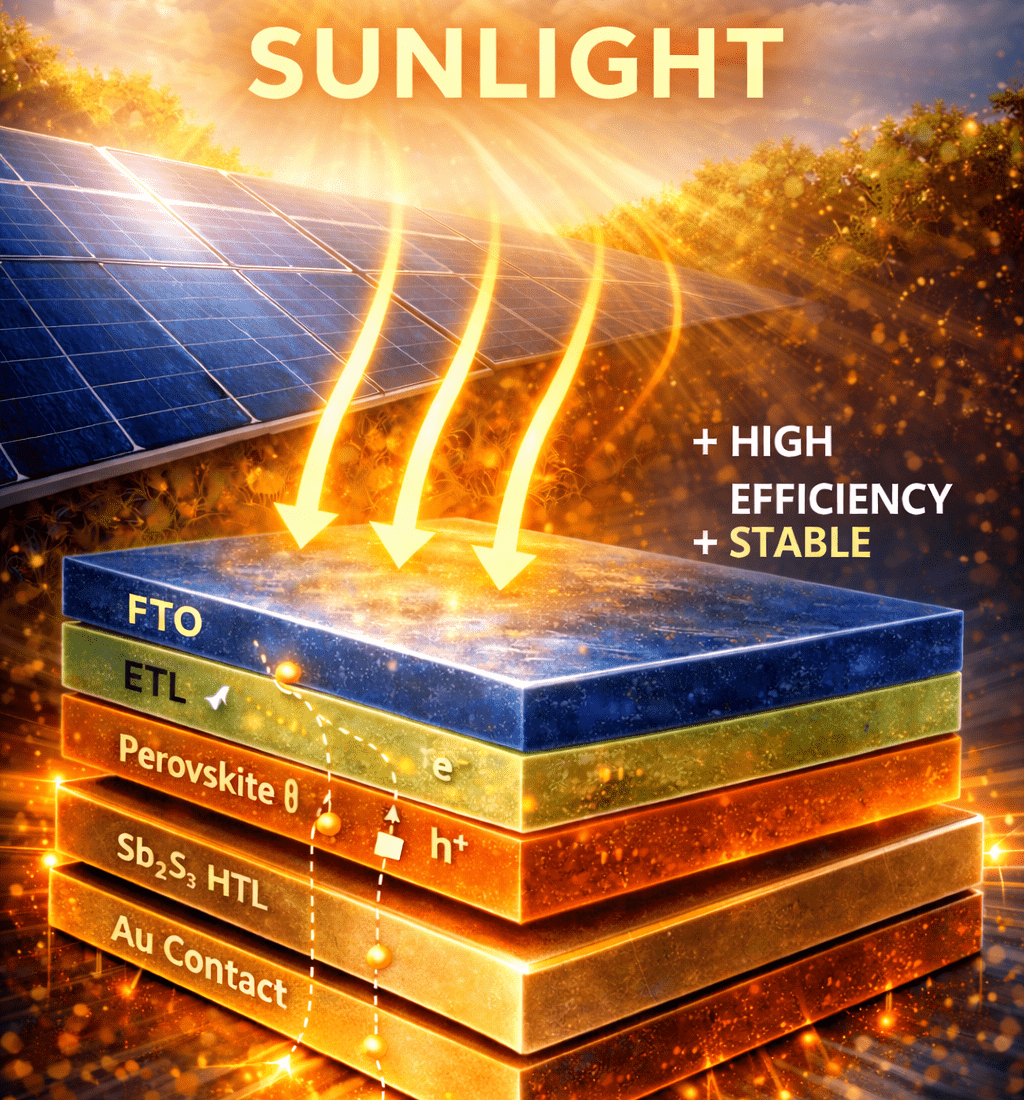
Why transport layers matter in photovoltaic design
Inside a perovskite solar cell, several functional layers work together to control the movement of charge carriers. In addition to the light-absorbing perovskite layer, devices typically include an electron-transport layer and a hole-transport layer. These layers selectively extract electrons and holes while preventing recombination losses that reduce efficiency.
The electron transport layer directs electrons toward the front electrode, while the hole transport layer carries positively charged carriers toward the back contact. Efficient transport layers, therefore, play a critical role in determining overall photovoltaic performance.
Conventionally, materials such as Spiro-OMeTAD and PEDOT:PSS have been widely used as hole-transport layers in perovskite solar cells. However, these organic compounds often suffer from several drawbacks. They can be hygroscopic, meaning they absorb moisture from the environment, and they may require chemical dopants to improve conductivity. Such characteristics can compromise device stability and increase production costs.
Exploring the potential of antimony trisulfide
Antimony trisulfide has attracted attention in photovoltaic research because of its favourable electronic properties and chemical stability. With a bandgap of around 1.7 electron volts and strong optical absorption, the material can efficiently transport holes while blocking electron backflow. Moreover, antimony and sulphur are relatively abundant elements, which could support cost effective large scale production.
To examine the potential benefits of this material, the research team conducted a detailed numerical simulation using the Solar Cell Capacitance Simulator (SCAPS)-1D solar cell modelling software. The simulated device structure consisted of several layers arranged as fluorine doped tin oxide, strontium titanate, CH3NH3SnI3 perovskite absorber, Sb2S3 hole transport layer and a gold back contact.
Strontium titanate was selected as the electron transport layer because of its favourable electron mobility and compatibility with the perovskite absorber. The design aimed to optimise energy band alignment across the device interfaces, thereby reducing recombination losses and improving efficiency.
Understanding band alignment and charge transport
One of the most critical aspects of solar cell design is the alignment of energy bands at the interfaces between different materials. Improper band alignment can create barriers that hinder charge transport or promote recombination of electrons and holes.
The study examined conduction and valence band offsets at the interface between the perovskite absorber and the hole-transport layer. A carefully tuned valence band alignment facilitates efficient hole extraction while blocking electrons from flowing in the wrong direction.
The researchers found that the Sb2S3 based design exhibited a more favourable energy band configuration compared with devices using the conventional Spiro OMeTAD layer. Specifically, the valence-band offset at the interface enabled efficient hole transport into the transport layer while suppressing recombination. This improved band alignment contributes directly to enhanced photovoltaic performance.
Simulated efficiency gains
The simulation results revealed significant improvements in several key performance parameters when Sb2S3 replaced the conventional hole-transport layer. The open circuit voltage increased from approximately 1.11 volts to around 1.19 volts, indicating reduced recombination and stronger internal electric fields within the device.
Similarly, the short circuit current density rose from about 28.85 milliamperes per square centimetre to roughly 33.62 milliamperes per square centimetre. This increase reflects more efficient light absorption and improved charge carrier collection.
The fill factor also improved slightly, reaching approximately 89.5 percent. When combined, these enhancements produced a simulated power conversion efficiency of around 36 percent. Such performance represents a substantial improvement over the reference solar cell design based on Spiro-OMeTAD, which achieved an efficiency of approximately 28.5 percent in the same simulation environment.
The influence of defects and material thickness
Beyond basic performance metrics, the study also explored how structural parameters influence device behaviour. The researchers investigated the impact of absorber layer thickness, defect density and transport layer thickness on photovoltaic performance.
Increasing the thickness of the perovskite absorber generally enhances light absorption, thereby boosting current generation. However, excessively thick layers may also increase bulk recombination if charge carriers cannot reach the electrodes efficiently. The simulations indicated that an absorber thickness of approximately 1000 nanometres provided an optimal balance between absorption and carrier transport.
Stability and diode characteristics
Another important indicator of solar cell quality is the behaviour of the device under dark conditions. The researchers analysed dark current density across a range of temperatures to evaluate recombination and carrier injection processes.
The simulated device exhibited extremely low dark current density at zero bias, around 10⁻¹⁰ milliamperes per square centimetre at 300 kelvin. Such low leakage currents indicate a high quality junction with minimal interfacial defects and suppressed recombination losses.
Compared with previously reported perovskite solar cell designs, the proposed architecture showed significantly lower dark current. This suggests improved diode characteristics and enhanced thermal stability, both of which are critical for reliable long-term photovoltaic operation.
Innovating high-performance and durable solar cell technology is not just scientific progress; it is a commitment to the energy needs of future generations.
— Anuj K. Sharma
Reference
Chauhan, S., Sharma, A. K., Singha, N. S., & Prajapati, Y. K. (2026). Sb₂S₃ as hole transport layer material massively enhances the performance and stability of tin based perovskite solar cell. Journal of Electronic Materials, 55, 483 to 496. https://doi.org/10.1007/s11664-025-12519-w
Coauthors

Anuj K. Sharma is an associate professor of physics at the National Institute of Technology Delhi, India. He earned his MSc in physics from Indian Institute of Technology (IIT) Roorkee (2001) and PhD in physics from IIT Delhi (2006). He has also been a recipient of the Alexander von Humboldt fellowship (Germany) during 2007-08. He has published more than 145 research articles in international journals. He is associate editor of Optical Fiber Technology (Elsevier) and Frontiers in Electronic Materials, and is on the editorial board of Advanced Metamaterials (Springer). His research interests include optical sensors and photodetectors, plasmonics in thin-film and grating structures, fiber optics, nanophotonics, and optical device modeling.

Nitin S. Singha received the M.Tech. degree in Communication Systems and Networks from the National Institute of Technology Hamirpur, India, where he was a Gold Medalist, and a Ph.D. degree in Electrical Engineering from Indian Institute of Technology Kanpur in 2018. He has published more than 15 research papers in reputed international journals and IEEE Transactions.