
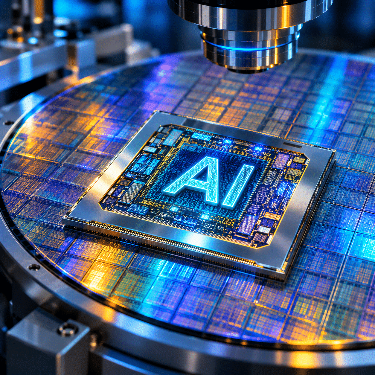
Artificial intelligence may appear to exist in the cloud, but behind every generated answer, image, prediction or scientific simulation lies an extraordinary piece of physical engineering: the semiconductor chip. These devices, often no larger than a fingernail, contain billions of microscopic electronic components that process information at remarkable speeds.
Few companies have brought semiconductors into public discussion as successfully as NVIDIA, founded by Jensen Huang in 1993. Once widely associated with graphics cards for computer gaming, the company has become a central supplier of processors for developing and operating modern artificial intelligence systems. Its graphics processing units, or GPUs, are now important components of data centres, scientific computing facilities and advanced computing infrastructure.
Yet the story of NVIDIA chips extends far beyond one technology company. It involves the physics of silicon, the chemistry of semiconductor manufacturing, highly specialised industrial equipment, international supply chains and geopolitical competition. It also raises questions about the energy, water and materials required to sustain the expanding AI industry.
Understanding NVIDIA, therefore, requires following the journey of a semiconductor from its fundamental electronic properties to the complex global system that designs, manufactures, packages, and uses it.
What exactly is a computer chip?
A computer chip, formally known as an integrated circuit, is a small electronic device containing interconnected components fabricated on a semiconductor material. Silicon is the most widely used material because its electrical properties can be controlled with remarkable precision. By introducing carefully selected impurities into silicon, manufacturers can modify its electrical conductivity.
The most important building blocks of modern computer chips are transistors. These microscopic electronic switches regulate the flow of electrical current. A transistor can represent two basic states, conventionally interpreted as binary 0 and 1. By combining billions of transistors into complex circuits, engineers create processors capable of performing calculations, storing information and controlling electronic systems.
Modern advanced processors contain billions of transistors, arranged into functional units that perform arithmetic, manage memory and communicate with other components. Their performance depends not simply on the number of transistors, but also on their architecture, operating frequency, energy efficiency, memory bandwidth and the software that controls them.
NVIDIA’s processors are designed around this principle. They combine large numbers of processing elements with specialised hardware and software to accelerate computational tasks. Their importance has grown because many modern scientific and artificial intelligence workloads require enormous numbers of mathematical operations to be performed efficiently.
Why does artificial intelligence need NVIDIA GPUs?
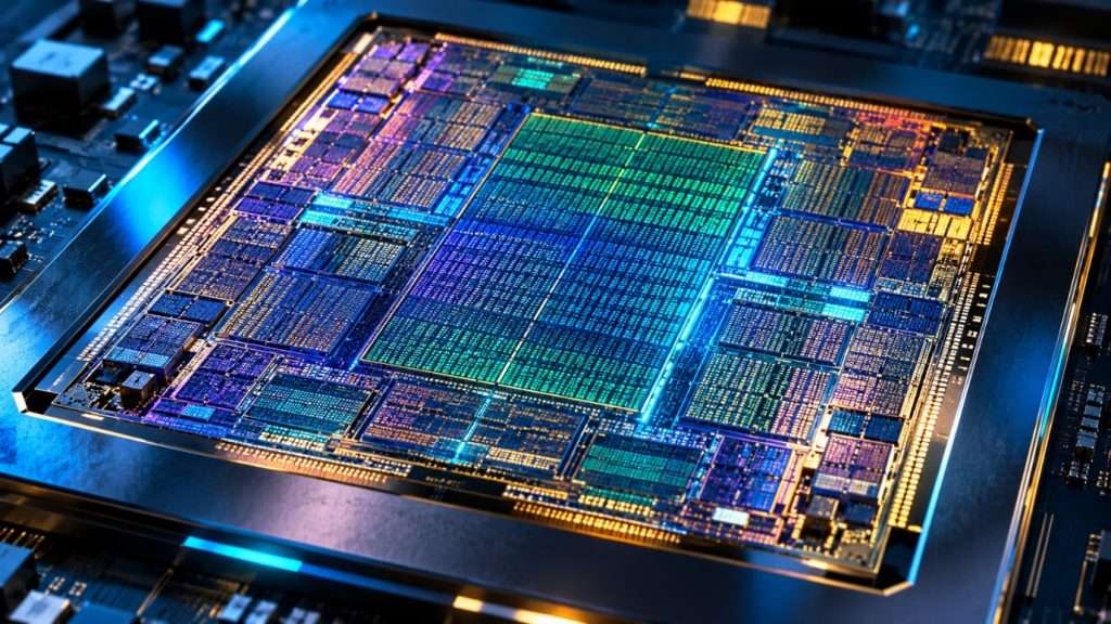
A central reason for NVIDIA’s influence is the suitability of graphics processing units for parallel computing. Traditional central processing units, or CPUs, are designed to handle a wide variety of tasks. They generally contain a relatively small number of sophisticated processing cores, making them effective at executing complex instructions and managing diverse operations.
GPUs use a different architectural approach. They contain many processing units designed to perform large numbers of similar calculations simultaneously. This parallelism was originally developed to render graphics, where millions of pixels and geometric operations must be processed efficiently. The same capability is highly valuable for artificial intelligence.
Deep learning models rely heavily on matrix multiplication and other tensor operations. A neural network, for example, repeatedly applies mathematical transformations to numerical data as information moves through its layers. During training, the model calculates errors and adjusts its parameters through processes such as backpropagation and gradient-based optimisation.
These calculations can involve billions or even trillions of numerical operations. GPUs can distribute much of this work across multiple processing units, reducing the time required for model training and inference. NVIDIA’s Tensor Cores are specialised hardware units designed to accelerate matrix and tensor calculations used in AI workloads.
However, the hardware is only part of the explanation. NVIDIA has also developed a software ecosystem centred on CUDA, its parallel computing platform and programming model. CUDA allows developers to write software that uses GPU resources for applications ranging from deep learning to scientific simulation. This combination of hardware, libraries, development tools and established software support has helped create a substantial advantage for the company.
What goes into making an advanced semiconductor?
The manufacturing of an advanced semiconductor begins with exceptionally pure materials. Silicon is extracted from silica-rich sources, purified and processed into a single-crystal ingot. The ingot is sliced into thin wafers, which are polished to produce extremely smooth surfaces suitable for fabricating microscopic electronic structures.
Silicon is not the only material involved. Semiconductor manufacturing uses a complex combination of metals, dielectric materials, gases and specialised chemicals. Copper and tungsten are used in electrical interconnections, while silicon dioxide, silicon nitride and other insulating materials help separate and protect different components. Advanced transistor structures may also incorporate materials such as hafnium oxide.
The manufacturing process requires carefully controlled chemical reactions and surface treatments. Depending on the process stage, manufacturers may use gases such as nitrogen, argon, hydrogen and silane, alongside chemicals including hydrofluoric acid, hydrogen peroxide and sulphuric acid. These substances have different functions, from cleaning and etching to depositing or modifying thin films. Not every chemical is used in every fabrication process.
The objective is to construct extraordinarily small electronic structures with precise electrical characteristics. Even microscopic contamination or a minor manufacturing defect can affect the performance and reliability of a chip. Semiconductor fabrication facilities therefore operate under stringent cleanroom conditions, with tightly controlled temperature, humidity, airborne particles and chemical purity.
How are NVIDIA AI chips manufactured?
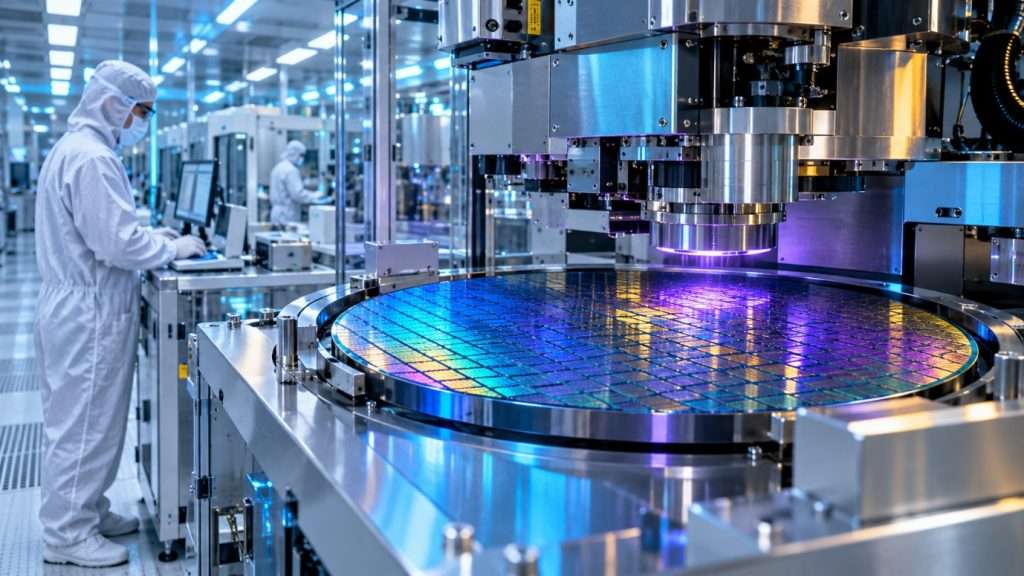
Advanced semiconductor manufacturing involves hundreds, or in some cases thousands, of carefully controlled processing steps. One of the most important is photolithography (done at ASML in the Netherlands), which transfers intricate circuit patterns onto a silicon wafer.
During this process, the wafer is coated with a light-sensitive material called photoresist. A lithography system exposes selected regions to light through a patterned mask. The exposed or unexposed regions are then developed, depending on the photoresist chemistry, creating a pattern that can guide subsequent etching or deposition processes.
One particularly important technology is extreme ultraviolet lithography, commonly known as EUV. It uses light with a wavelength of 13.5 nanometres to print extremely small features on semiconductor wafers. EUV systems are particularly important for manufacturing some of the most advanced logic and memory chips.
Lithography is only one part of the process. Etching removes selected material, while deposition techniques such as chemical vapour deposition and atomic layer deposition create extremely thin films. Doping introduces controlled impurities to modify the electrical properties of silicon. Chemical mechanical planarisation, or CMP, smooths the wafer surface between processing stages.
These operations are repeated to create transistors and the complex network of electrical connections that links them. Once fabrication is complete, the wafer undergoes testing before being cut into individual dies. The dies are then packaged to protect them and provide electrical connections to the outside world.
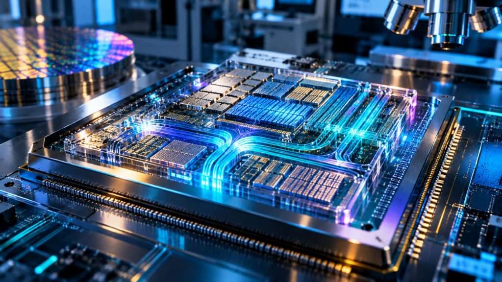
For advanced AI processors, packaging has become increasingly important. High-bandwidth memory, or HBM, can be integrated with processor dies using advanced packaging technologies. This reduces the distance that data must travel and supports the high memory bandwidth required by demanding AI workloads. Technologies such as TSMC’s Chip on Wafer on Substrate (CoWoS) are part of this advanced packaging landscape.
Does NVIDIA manufacture its own chips?
Despite its central position in the semiconductor industry, NVIDIA does not operate as a conventional manufacturer that fabricates all its own advanced processors. It primarily follows a fabless business model. This means that the company designs its chips and associated computing platforms, while specialist manufacturing partners produce the silicon.
One of its most important manufacturing partners is Taiwan Semiconductor Manufacturing Company, or TSMC. TSMC operates as a dedicated semiconductor foundry, manufacturing chips designed by other companies. Its facilities use highly advanced processes to produce processors for applications ranging from smartphones to high-performance computing.
Other companies play equally important roles in the supply chain. ASML, headquartered in the Netherlands, is the world’s leading supplier of EUV lithography systems. These machines are essential for producing many of the most advanced semiconductor structures. South Korean companies such as SK hynix and Samsung, alongside US-based Micron, are important suppliers in the high-bandwidth memory market.
The final processor is therefore the product of a highly interconnected industrial ecosystem. NVIDIA contributes chip architecture, system design and software. TSMC provides advanced wafer fabrication and packaging capabilities, while specialist suppliers provide lithography equipment, memory, materials and other essential components.
This division of expertise explains why semiconductor manufacturing is so difficult to replicate. A company cannot simply purchase silicon and build an advanced processor. It requires access to specialised machinery, intellectual property, chemical suppliers, highly trained engineers, precision manufacturing facilities and years of accumulated process knowledge.

Why is NVIDIA worth so much?
NVIDIA’s commercial success reflects more than the sale of individual graphics cards or processors. The company supplies a broader computing platform that includes GPUs, networking equipment, systems, software libraries and development tools. This integrated approach allows customers to purchase much of the infrastructure needed to build and operate large-scale AI systems.
Its CUDA software ecosystem is particularly significant. Developers and research institutions have spent years building applications around NVIDIA hardware and software. Moving to a competing platform can therefore involve more than replacing a processor. It may require adapting code, changing software libraries, retraining technical teams and validating performance across different systems.
The rapid expansion of generative AI has increased demand for data centre infrastructure. NVIDIA’s fiscal 2026 annual report recorded revenue of approximately US$215.9 billion, with its Data Centre business accounting for the largest share. This illustrates how strongly the company’s financial performance has become linked to investment in AI computing infrastructure.
Nevertheless, NVIDIA does not operate without competition. AMD develops Instinct accelerators, while Google designs Tensor Processing Units for its own AI infrastructure and cloud services. Intel also offers specialised data centre accelerators. Chinese companies, including Huawei, are developing domestic alternatives in response to technology restrictions and the strategic importance of computing hardware.
The competitive challenge is not simply to produce a chip with comparable processing performance. Alternatives must also offer reliable software, developer support, memory capacity, networking and access to large-scale manufacturing. NVIDIA’s position is supported by the interaction of these elements, although its long-term market position will depend on technological progress, customer choices, supply constraints and competition.
What is the environmental cost of AI chips?
The semiconductor industry is often associated with digital technology, but its manufacturing processes have substantial physical resource requirements. Fabrication facilities consume electricity, water, industrial gases and specialised chemicals. Their environmental footprint begins long before a processor is installed in a data centre.
Water is particularly important. Semiconductor fabrication requires ultrapure water to clean wafers and remove microscopic contaminants during repeated manufacturing stages. Ordinary drinking water is not sufficiently pure for these applications. It must undergo extensive treatment to remove dissolved ions, organic compounds, particles and microorganisms.
A 2023 study examining environmental data from 28 semiconductor corporations highlighted the scale of these resource demands. It reported total water withdrawal of approximately 789 million cubic metres, energy consumption of around 149 billion kilowatt-hours and greenhouse gas emissions of approximately 71.5 million tonnes of carbon dioxide equivalent across the companies surveyed for 2021. The study also estimated global ultrapure water consumption at approximately 551 million cubic metres in 2022. These figures describe the industry-wide data examined by the researchers, not the footprint of an individual chip or NVIDIA product.
Energy consumption is another major concern. Semiconductor fabrication facilities require continuous operation of cleanrooms, ventilation systems, process equipment and water treatment infrastructure. Some industrial gases used in manufacturing also have high global warming potentials if released into the atmosphere. Effective abatement systems, careful chemical management and process optimisation are therefore essential.
The environmental impact does not end when a chip leaves the factory. AI data centres consume electricity to operate processors, networking systems and cooling equipment. Their water footprint can also include direct cooling requirements and the water used to generate electricity. It is important to distinguish the environmental impacts of semiconductor fabrication from those of operating AI infrastructure, even though both contribute to the wider footprint of artificial intelligence.
The industry’s sustainability challenge is consequently twofold: reducing the resources needed to manufacture advanced chips and improving the energy and water efficiency of the computing systems that use them. Renewable electricity, water recycling, process optimisation, low-emission gases and improved cooling technologies will all influence the environmental performance of future AI infrastructure.
What could replace silicon in future computer chips?
Silicon has been the foundation of modern electronics for decades, but researchers are investigating materials and architectures that could extend computing performance beyond conventional semiconductor scaling. As transistor dimensions become increasingly small, controlling heat, electrical leakage, power consumption and manufacturing complexity becomes more difficult.
Graphene is one material attracting attention because of its exceptional electrical conductivity, mechanical strength and thermal properties. However, pristine graphene does not naturally possess the bandgap required for conventional digital switching. This makes it challenging to use as a direct replacement for silicon in standard logic transistors. Researchers are exploring ways to engineer its electronic properties, but substantial technical barriers remain.
Other materials are already transforming specific areas of electronics. Gallium nitride and silicon carbide are wide-bandgap semiconductors that can operate at high voltages, temperatures and switching frequencies. They are particularly valuable in power electronics, electric vehicles, renewable energy systems and efficient power conversion. Their role is complementary to silicon in many applications rather than a straightforward replacement for the processors used in AI data centres.
Silicon photonics offers another possible direction. Instead of relying entirely on electrical signals to transmit information, photonic technologies use light to move data. Optical communication can support high bandwidth and potentially reduce some energy and latency constraints in data centre networks. This is especially relevant as AI systems increasingly depend on communication between large numbers of processors.
Researchers are also investigating neuromorphic computing, which seeks to mimic aspects of biological neural systems, and quantum computing, which uses quantum mechanical effects to process information. Neither should be understood as an imminent universal replacement for GPUs. Quantum computers are designed for particular classes of problems, while neuromorphic systems remain an evolving research area. Future computing is more likely to involve several complementary technologies than one material or architecture replacing all others.

How are NVIDIA GPUs changing science and medicine?
The influence of GPU computing extends well beyond chatbots and commercial AI applications. Scientific research increasingly relies on computational methods to investigate systems that are too complex, expensive or time-consuming to study through experiments alone. High-performance GPUs can accelerate simulations, numerical modelling, image processing and machine learning.
In drug discovery, GPU-accelerated computing can support molecular dynamics simulations, molecular docking and virtual screening. Researchers can investigate how potential drug molecules interact with biological targets, explore protein structures and prioritise compounds for laboratory testing. These computational approaches do not replace experimental validation, but they can help narrow the search space and guide research decisions.
In medicine, AI systems can analyse medical images, identify patterns in large clinical datasets and support selected diagnostic workflows. Their performance depends on the quality of training data, clinical validation and integration into healthcare practice. A powerful GPU does not automatically produce a reliable medical tool. Scientific evidence, responsible data governance and professional oversight remain essential.
GPU computing is also valuable in environmental science, climate modelling, materials research and computational chemistry. Researchers can simulate chemical reactions, investigate the properties of new materials, model pollutant transport and analyse complex environmental datasets. Such applications are relevant to fields ranging from renewable energy and battery development to water treatment and contaminant monitoring.
The wider research ecosystem is already exploring how artificial intelligence is evaluated and applied in scientific and societal settings. Readers can explore related coverage in The Science Matters articles on artificial intelligence systems and increasingly complex examinations and the changing relationship between artificial intelligence and human judgement. These developments highlight that computing power is only one part of the transformation. The quality of the scientific questions, data and methods remains just as important.
References
- Huang, J., et al. (2023). Environmental data and facts in the semiconductor manufacturing industry: An unexpected high water and energy consumption situation. Water Cycle, 4, 47–54. https://doi.org/10.1016/j.watcyc.2023.01.004
- NVIDIA, CUDA programming guide. NVIDIA Documentation. https://docs.nvidia.com/cuda/cuda-programming-guide/
- ASML, EUV lithography systems. https://www.asml.com/en/products/euv-lithography-systems
- Taiwan Semiconductor Manufacturing Company. (2026). 2025 annual report. https://investor.tsmc.com/static/annualReports/2025/english/index.html
- NVIDIA Corporation. (2026). 2026 annual report. https://s201.q4cdn.com/141608511/files/doc_financials/2026/ar/2026-Annual-Report-Web.pdf